

TechnologyMarch 19, 2023
High-channel density digital IO modules for factory automation

From a heat, reliability, and size considerations, an integrated device option must be carefully considered. When choosing integrated DI or DO devices, the robust operating specifications, diagnostics and the support of multiple input-output configurations are some of the important data points to keep in mind.
There is a lot of ink spilled on Industry 4.0 and the rising ubiquity of intelligent sensors on the factory floor. While sensor proliferation is something we clearly see in factories, process plants, and even in newer building automation systems, one important change this ubiquity of sensors necessitates is the requirement to process a large number of IOs within typically the same old controller form-factor. The IOs can be digital or analog. This requires architecting a high-density IO module with size and heat constraints. I will focus on the digital IOs in this article and take on the analog IOs in a subsequent piece.

Typically, the digital IOs in PLCs were conditioned using discretes like resistors/capacitors or driven using individual FETs. The need to minimize the footprint of the controllers along with the real requirement of being able to process 2x to 4x the number of channels are pushing a move away from discrete implementation to an integrated approach.
Considerations for digital input and output modules.
| Digital INPUT | DIGITAL OUTPUT |
|---|---|
| Size | Support for different types of output driver configuration |
| Heat | Size – Integrated demagnetization of inductive load |
| Support for all input types – Type 1, 2, 3 input – Support for 24V and 48V input |
Heat — when driving multiple outputs |
| Robust operating specifications | Drive accuracy |
| Wire break detection | Diagnostics |
We could spend this entire article talking about the disadvantages of a discrete approach, especially when the number of channels being processed per module is eight or higher – but suffice it to say that high heat/power dissipation, the unwieldy number of discrete parts required (both from a size and a (Mean Time Between Failure) MTBF perspective) and the need to have a rugged system specification have almost completely rendered the discrete approach unworkable.
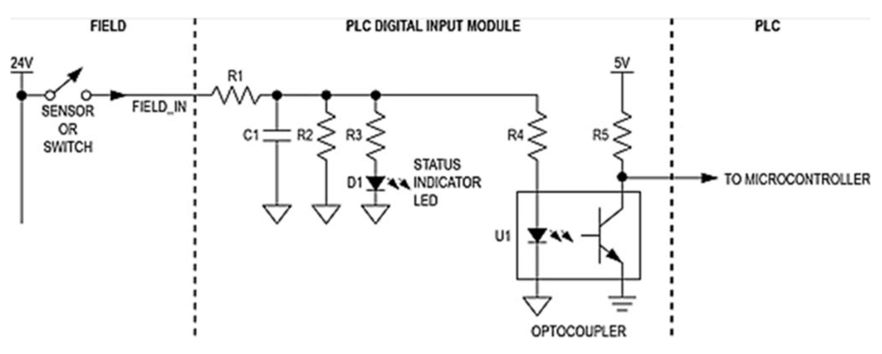
A traditional digital input design using discrete logic.
The table above shows the technical challenges of architecting a high-density digital input (DI) and digital output (DO) modules. Size and heat are considerations in both Di and DO systems.
For digital inputs, it is also important that different types of inputs are supported – both types (type 1,2,3) of inputs and, in some cases, 24V and 48V inputs. In all cases, robust operating specifications are very important and sometimes wire break detection is crucial.
For digital outputs, systems use different FET configurations to drive the load. The accuracy of the drive current is generally an important consideration. And in many cases, diagnostics are important.
We will discuss how an integrated solution can help with some of these challenges.
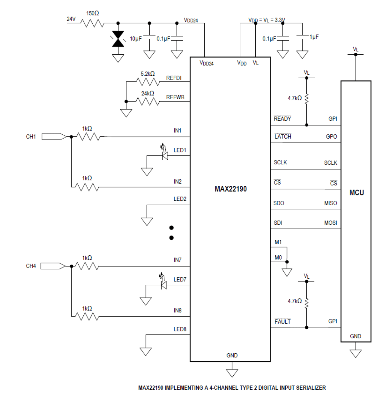
Using 2-channels in parallel to support a type 2 digital input.
Designing a High-Channel Density Digital Input Module
A traditional discrete design uses a resistor divider network to convert a 24V/48V signal to something a microcontroller can use. There can be a discrete RC filter at the front as well. If isolation is a requirement, an external optocoupler is sometimes used. The figure illustrates a typical discrete approach to implement a digital input circuit.
This type of design is good for up to a certain number of digital inputs; say 4 to 8 per board. Any number beyond that and it rapidly becomes impractical. The different issues with such a discrete implementation include:
- High power consumption and associated board hot spots.
- One optocoupler needed for each individual channel.
- Too many components resulting in low FIT rate and even requiring a larger form-factor.
Most importantly, a discrete design approach means the input current increases linearly with input voltage. Assume a 2.2KΩ input resistor and 24V VIN. When the input is 1, i.e., at 24V, the input current is 11mA, which equates to power consumption of 264mW. For an 8-channel module, the power consumption is over 2W and for a 32-channel module, the power consumption is over 8W.
Purely from a heat perspective, this discrete design cannot support multiple channels on a single board.
One of the biggest advantages of an integrated digital input design is significantly lower power consumption and thus heat dissipation. Most integrated digital input devices allow for configurable input-current limiting, dramatically reducing power consumption.
With current limit set to 2.6mA, the power dissipation is reduced significantly to approximately 60mW per channel. An 8-channel digital input module can now be rated at under half a watt as shown.
| # of DI Channels | Estimated Power Consumpton |
|---|---|
| 8 | 2.1 W |
| 16 | 4.2 W |
| 32 | 8.4 W |
| 64 | 16.9 W |
Another reason going against a discrete logic implementation is that sometimes DI modules must support different types of inputs. The standard 24V digital input specification published by the IEC is divided into types 1, 2, and 3. Types 1 and 3 are generally lumped together as the current and the threshold limits are very similar. Type 2 has a 6mA current limit, which is much higher. With a discrete approach, this would require a redesign since most discrete values would need to be updated.
However, integrated digital input products can typically support all these three types. Natively, types 1 and 3 are always supported by integrated digital input devices. However, to meet the minimum 6mA current requirement for type 2 inputs, we need to use two channels in parallel for one field input. And just adjust the current limit resistors. There would be a board change, but it is minimal.
For example, the current Maxim Integrated DI devices have a current limit of 3.5mA/channel. So, as shown, we would use two channels in parallel and adjust the REFDI resistor and the RIN resistors if the system must interface with type 2 inputs. For some of the newer parts, we can also select the current value using a pin or through software.
To support a 48V digital input signal (not a very common requirement) would require a similar process where one would have to add an external resistor to adjust the field side voltage threshold. The value of this external resistor is set so that Current limit * R + threshold at pin meets the field side voltage threshold specification (defined in the data sheet of the device).
| # of DI Channels | ESTIMATED POWER CONSUMPTON (DISCRETE APPROACH) |
ESTIMATED POWER CONSUMPTON (DISCRETE APPROACH) |
|---|---|---|
| 8 | 2.1 W | 0.48 W |
| 16 | 4.2 W | 0.96 W |
| 32 | 8.4 W | 1.92 W |
| 64 | 16.9 W | 3.84 W |
Finally, since digital input modules are interfacing with sensors, they must be designed to robust operating specifications. When implemented using discretes, these protections must be carefully designed. When choosing integrated digital input devices, ensure these come with these industrial-ready specifications:
- Wide Input voltage range (up to 40V for example).
- Ability to operate from field supply (7V to 65V).
- High ESD (±15kV ESD Air Gap) and surge tolerant (typically 1KV).
It is also very useful to have over voltage and over temperature diagnostics so that the MCU can take appropriate action.
Designing a High-Channel Density Digital Output Module
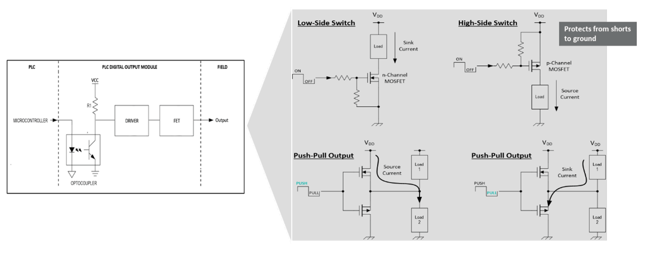
A typical discrete digital output design features a FET with drives circuitry driven by the microcontroller. There are different ways of configuring the FET to drive the microcontroller.
The definition of a high-side load switch is that it is controlled by an external enable signal and connects or disconnects a power source to a given load. Compared to a low-side load switch, a high-side switch sources current to the load, while the low-side type connects or disconnects the load to ground, and therefore sinks current from the load. While they both use a single FET, the problem with the low-side switch is that the load could get shorted to the ground. High-side switches protect the load from shorts to ground. But the low-side switch implementation is marginally lower cost. Sometimes output drivers are also configured as push-pull that requires two MOSFETs. See the following Figure 6:
A configurable DI/DO product for a 4-channel implementation.
Integrated DO devices can incorporate multiple DO channels in a single device. Since the FET configuration is different for high-side, low-side, and push-pull, different devices are available to implement each type of an output driver.
Built-In Demagnetization for Inductive Loads
One of the key advantages of an integrated digital output device is that demagnetization for inductive loads is built-in to these devices.
An inductive load is any device that has coils of wire, which when energized, generally perform some mechanical work, for example solenoids, motors, and actuators. The magnetic field caused by the current flow can move the switching contacts in a relay or contactor, operate solenoid valves, or rotate a shaft in a motor. Mostly, engineers use a high-side switch to control the inductive load, and the challenge is how to discharge the energy in the inductor when the switch opens, and the current is no longer sourced to the load. The negative impacts of not discharging this energy correctly include potential arcing of relay contacts, large negative voltage spikes damaging sensitive ICs, and the generation of high frequency noise or EMI that can affect system performance.
In a discrete implementation, the most common solution to discharge the inductive load uses a free-wheeling diode. In this circuit, while the switch is closed, the diode is reverse-biased and does not conduct any current. When the switch opens, the negative voltage across the inductor forward biases the diode, allowing the stored energy to decay by conducting the current through the diode until steady state is reached and the current is zero.
For many applications, especially those found in industrial applications that have many output channels per IO card, this diode is often physically quite large and adds significant extra cost and size to the design.
Modern digital output devices implement this function within the device using a kind of active clamping circuitry. For example, Maxim Integrated implements a patented safe demagnetization (SafeDemagTM) feature that allows our digital-output devices to safely turn off loads with unlimited inductance.
More details are available in an application note on Maxim Integrated’s website: https://www.maximintegrated.com/en/design/technical-documents/app-notes/6/6307.html
There are many important factors when selecting a digital output device. Some of the following data sheet specifications should be considered carefully:
- Look at the maximum continuous current rating and ensure that if needed, you can parallel multiple outputs to get a higher current drive.
- Ensure the output device can drive multiple channels with high currents (over the temperature range). Refer the data sheet specifications to ensure the on-resistance, supply current, and thermal resistance values are as low as possible.
- The output current drive accuracy specification is also important.
Diagnostic information is also essential to recover from some out-of-range operating conditions. First, you want diagnostic information reported per output channel. This will be temperature, overcurrent, open, and shorts. On a global (chip) basis, some important diagnostics are thermal shutdown, VDD undervoltage, and SPI diagnostics. Look for some or all of this in the integrated digital output device.
Programmable Digital Input/Output Device
Once we start integrating DI and DO on an IC, it allows us to build products that are configurable. An example is a 4-channel product that can be configured as an input or an output.
This has a DIO core, which means a single channel can be configured as a DI (type 1/3 or type 2) or a digital output in either a high-side or in a push-pull mode. The current limit on the DO can be set from 130mA to 1.2A. Demagnetization is built-in. To switch between type 1/3 or type 2 digital inputs, we only need to set a pin and no external resistors are needed.
These devices are not only very configurable but also ruggedized to work in an industrial setting. This means high ESD, supply voltage protected up to 60V and line to ground surge protection. This is an example of something completely different (a configurable DI/DO module) possible with an integrated approach.
Conclusion
Once you are designing a high-density digital input or output module, it becomes clear that beyond a certain channel density a discrete implementation does not make a lot of sense. From a heat, reliability, and size considerations, an integrated device option must be carefully considered.
When choosing integrated DI or DO devices, the robust operating specifications, diagnostics, and the support of multiple input-output configurations are some of the important data points to keep in mind.